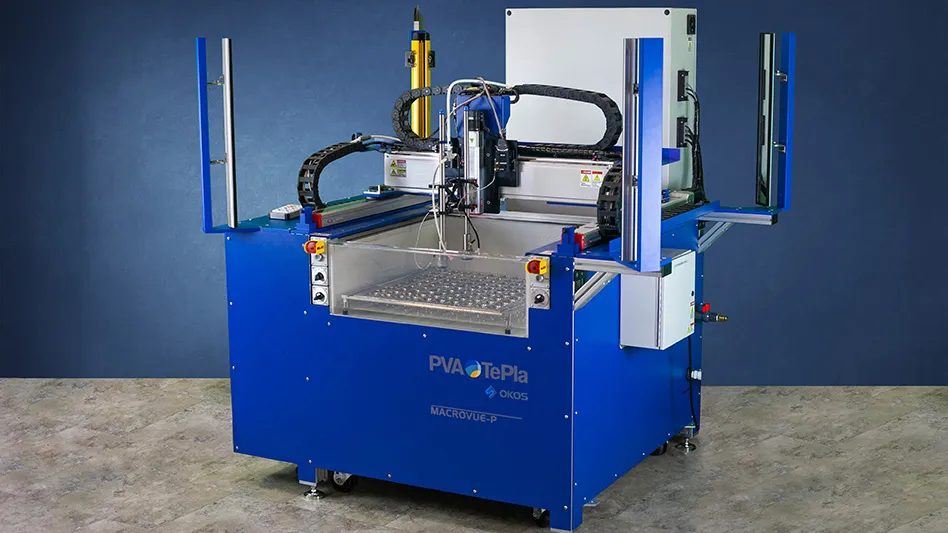
Courtesy of OKOS
To meet ever increasing demand for silicon carbide (SiC) crystals, the world needs much higher yields without sacrificing quality. Today, SiC crystals are crucial in the manufacture of smaller, faster, more efficient chips and power electronics systems. However, without advanced metrology tools capable of promptly detecting minor flaws, the SiC crystal growing sector essentially operates blindly, resulting in unacceptable defects and costly product losses.
There is great complexity and secrecy in growing quality SiC crystals, and production is time-consuming. Growing a single crystal ingot, known as a boule, can take a few weeks to produce. Some of the variables in the process include the type of “seed,” powder, and equipment used as well as the temperatures and hot zones utilized to transfer the powder in gaseous form to the boule.
When dealing with new technologies such as SiC crystal production, a learning curve emerges, necessitating the use of sophisticated metrology tools to ensure consistent high-quality output throughout all production stages, from raw materials to the final product.
After all, high-purity silicon carbide powder suppliers must ensure the reliability of their product; crystal growers cannot risk weeks of work resulting in flawed products; and semiconductor manufacturers must avoid slicing boules into defective wafers used to create advanced chips, EVs, and electronics.
With the silicon carbide production industry still in its nascent stages, those driving innovation to achieve a competitive edge and deliver high-yield, reliable products must conduct defect testing throughout all production phases. Utilizing advanced metrology methods, such as Scanning Acoustic Microscopy (SAM), becomes crucial for defect identification, elimination, and process optimization.
SAM, a non-invasive, non-destructive, ultrasonic testing method capable of highspeed 100% testing, is already the industry standard for 100% inspection of semiconductor components for identifying defects within microelectronic devices.
“If the final product cannot be inspected, it becomes challenging to identify potential imperfections in the SiC crystals and pinpoint the stage of the process where issues may have arisen. Possible causes could include material defects, temperature fluctuations, or problems within the hot zone. Advanced metrology equipment like SAM can help crystal growers detect minute flaws, defects, and map these [into their process variation] to correct any problems going forward,” says Hari Polu, President of OKOS, a Virginia-based manufacturer of SAM and industrial ultrasonic non-destructive (NDT) systems. The company serves the SiC crystal growing, chip fabrication, electronics, aerospace, metal/alloy/composite manufacturing, and end-user markets.
SAM enables rapid, high-resolution SiC defect detection
SiC stands as a highly promising material for electronic devices with high temperature, high frequency, and high-power requirements. Nevertheless, the commercialization of numerous SiC-based electronic devices encounters challenges due to various extended defects.
An essential consideration for the practical use of SiC devices pertains to challenges associated with the quality of SiC wafer crystals. During the growth of SiC crystals, localized disruptions in structural uniformity occur, leading to crystal defects like stacking faults and dislocations. It is widely acknowledged that certain defects have a detrimental impact on device functionality.
To increase the yield and reliability of SiC devices, it is therefore important to identify potential defects through advanced metrology systems like SAM. Recent advances in SAM also facilitate the detection of much smaller defects than previously possible.
“Advanced SAM systems make it possible to move to a higher level of failure analysis because of the level of detection and precision involved. In the past, detecting a 500-micron defect was the goal; now it is a 50-micron defect. With this type of testing, we can inspect materials and discover flaws that were previously undetected,” says Polu.
In fact, SAM seems to address at least one of the elements identified by the National Institute of Standards and Technology (NIST) as necessary for the U.S. to lead the global semiconductor manufacturing industry once again.
NIST’s recent report titled Strategic Opportunities for U.S. Semiconductor Manufacturing identifies 7 Grand Challenges that need critical attention from a metrology perspective to achieve the vision of a U.S.-led global semiconductor industry. In addition, the report identifies 32 Path Forward Elements that describe potential strategies for addressing the challenges.
For one of the grand challenges, Advanced Metrology for Future Micro-electronics Manufacturing, SAM essentially answers one of the Path Forward Elements, namely “rapid, high-resolution, non-destructive techniques for characterizing defects and impurities and correlating them with performance and reliability.”
Scanning acoustic microscopy
Scanning acoustic microscopy (SAM) functions by directing focused sound from a transducer at a small point on a target object. The sound hitting the object is either scattered, absorbed, reflected, or transmitted. By detecting the direction of scattered pulses as well as the “time of flight,” the presence of a boundary or object can be determined as well as its distance.
To produce an image, samples are scanned point by point and line by line. Scanning modes range from single layer views to tray scans and cross-sections. Multi-layer scans can include up to 50 independent layers. Depth-specific information can be extracted and applied to create two-and three-dimensional images that can be analyzed to detect and characterize flaws such as cracks, inclusions, and voids.
Smaller manufacturers and independent testing labs are likely to have a tabletop SAM model that provides a scan envelope of over 300 mm with a maximum scan velocity of 500 mm/s and accuracy and repeatability of +/- 5.0 micron. Software allows using saved data to virtually re-scan, view, and analyze data for simultaneous real-time analysis or post collection review. Often, such tabletop units are used to analyze data for failure analysis, product inspection, quality control, R&D, process validation, as well as to determine product reliability, in process quality control, and vendor qualification.
As requirements rise to accommodate testing for higher levels of production, SiC crystal growers, silicon carbide wafer manufacturers, and semiconductor fabs will often utilize a larger system with the capability of high-speed inspection. The challenge, however, is to perform this inspection at extremely high throughput with 100% inspection to identify and remove SiC crystals or sliced wafers that do not meet quality requirements. This necessitates more advanced equipment that can simultaneously inspect several layers, often on multiple channels, scanning multiple samples in handling trays in an automated fashion to accelerate the process.
According to Polu, SAM can also be custom designed to be fully integrated into high volume manufacturing systems. Advanced inspection technologies detect minute flaws in SiC boules and semiconductor wafers for 100% inspection of all materials. So, SiC crystal growers and semiconductor fabs now have access to 100% inspection of SiC boules, wafers, panels, and singulated components in trays.
Recent advancements in SAM technology have also significantly improved throughput speeds and defect detectability. When high throughput is required for 100% inspection, ultra-fast single or dual gantry scanning systems are utilized along with multi-head transducers that can be used to simultaneously scan for higher throughput.
As important as the physical and mechanical aspects of conducting a scan, the software is critical to improving the resolution and analyzing the information to produce detailed scans.
Multi-axis scan options enable A, B, and C-scans, contour following, off-line analysis, and virtual rescanning of chips. This results in highly accurate internal and external inspection for defects and thickness measurement via the inspection software.
Various software modes can be simple and user friendly, advanced for detailed analysis, or automated for production scanning. An off-line analysis mode is also available for virtual scanning.
Polu estimates that OKOS’ software-driven model enables them to drive down the costs of SAM testing while delivering the same quality of inspection results. Consequently, this type of equipment is well within reach of even modest SiC testing labs.
“Every SiC crystal grower and semiconductor wafer producer will eventually move towards a higher level of failure analysis because of the stringent detection and precision requirements today,” says Polu. “The cost advantages and time savings of SAM equipment make this possible.”
With labs in Santa Clara, California, and Manassas, Virginia, OKOS offers contract analysis and testing services that meet existing industrial and military standards. The service also provides customers with the ability to vet technology and feasibility prior to investing in equipment.
Today, for the SiC crystal growers, chip fabricators, and component manufacturers ramping up production capacity for global demand, SAM offers the best value due to the exceptional level of defect and failure analysis detail it provides, compared to conventional methods. As a result, advanced SAM systems are now considered essential tools in SiC production facilities, R&D, and Quality Assurance labs.
Latest from EV Design & Manufacturing
- Archer completes installation of high-volume battery pack manufacturing line
- Siemens Xcelerator as a Service expands across the product lifecycle
- Lyten ships lithium-sulfur battery A-samples for automotive, consumer electronics, and military customer evaluation
- Latest advancements in machine tool technology
- Visit Okuma America at IMTS 2024
- Eaton to supply ELocker differential system to leading electric vehicle manufacturer
- AM for Aircraft Cockpit Interior Components
- Addionics and IL Science sign MOU to develop next-gen high-performance lithium metal batteries


